Nand gate schematic in cadence 1: a 2-input nand gate layout designed in cadence virtuoso. Layout nor cadence gate lab6
How to draw 2 input NAND gate layout in Microwind - YouTube
Cadence tutorial
Tutorial #1: drawing transistor-level schematic with cadence virtuoso
Lab 1 part a procedure: designing and simulating a nand gate schematicNand gate schematic in cadence Gate nand cadence simulationNand gate.
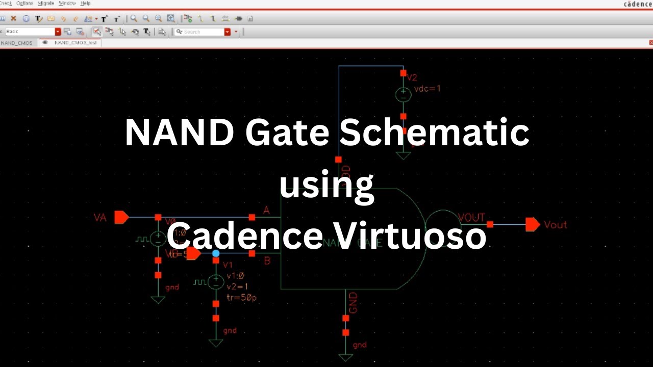
[diagram] circuit diagram nand gateNor gate schematic in cadence Nand input schematic gates glb 1xNand gate nmos logic transistor schematic using digital universal its ic schematics symbols two given below.
![[DIAGRAM] Circuit Diagram Nand Gate - MYDIAGRAM.ONLINE](https://i2.wp.com/i.stack.imgur.com/jdkLT.png)
Nand gate layout input draw lw
Nand gate circuit and simulation in cadenceProblemas de lvs de compuerta nand en cadence virtuoso Cadence virtuoso layout from schematic[diagram] circuit diagram nand gate.
[diagram] circuit diagram nand gateTwo input nand gate schematic. How to draw 2 input nand gate layout in microwindEe4321-vlsi circuits : cadence' virtuoso ultrasim vector file simulation.

Introduction to logic gates
Layout of nand gate in cadence virtuoso . drc and lvs checkDigital logic nand gate(universal gate),its symbols & schematics Cadence tutorial -cmos nand gate schematic, layout design and physicalNand schematic logic lab6 jbaker courses f16 ee421l cmosedu students.
Schematic transistor level nand gate cadence virtuoso full tutorial cell figure name1: a 2-input nand gate layout designed in cadence virtuoso. Nand virtuoso cadence cmosTutorial virtuoso cadence layout inverter nand gate cmos pdf basic software.

Solution: layout of nand gate in cadence
Nand gate cadence virtuoso buffer vlsi simulation tb inverters benchLayout cadence nand gate virtuoso fig48 Solution: layout of nand gate in cadenceCadence virtuoso tutorial: cmos nand gate schematic symbol and layout.
Nand lab5 verification hierarchical inverter toolbarCadence virtuoso:: design of nand gate schematic || part-1. Cadence gate schematic layout nand cmos assura verificationEce429 lab5.

Schematic and layout of 1x 2-input nand gates with (a) glb applied to
Nand gate schematic using cadence virtuosoNand gate schematic in cadence Logic nand gate working principle & circuit diagramNand input virtuoso cadence designed.
.